



Semiconductor manufacturers face a harsh reality: a single micron-level tolerance error can destroy entire production batches and cost thousands in rework. Traditional machining methods often fall short when creating the ultra-precise components that modern semiconductor equipment demands, leaving engineers scrambling for reliable solutions.
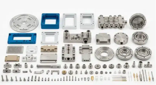
CNC machining provides semiconductor manufacturers with the precision, repeatability, and surface finish quality needed for critical components like housings, fixtures, and test equipment. This manufacturing method achieves tolerances as tight as ±0.0001 inches while maintaining consistent quality across production runs.
1.Why Semiconductor Manufacturers Can’t Afford Tolerance Errors
In the world of semiconductor manufacturing, there is no room for "almost right." Precision is everything. Even a deviation measured in microns, smaller than a human hair, can cause catastrophic failures.
This isn’t just about quality control. It’s about the fundamental physics that make modern electronics possible. Tight semiconductor machining tolerances are not a luxury; they are a baseline requirement.
The Cost of Inaccuracy
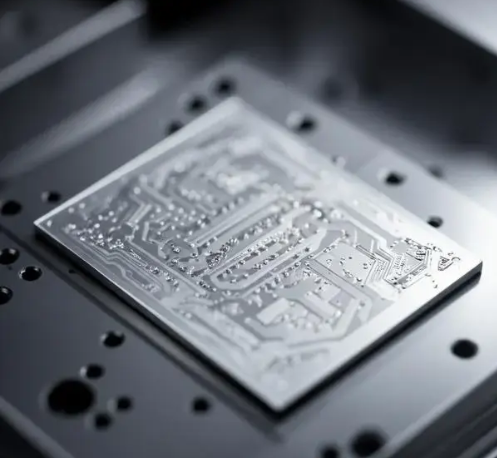 Even a minor slip in precision has huge costs. The impact goes beyond a single faulty component.
Tolerance Error | Consequence | Financial Impact |
1–2 Microns | Signal Integrity Loss | Moderate |
3–5 Microns | Overheating / Shorts | High |
5+ Microns | Complete Chip Failure | Critical |
The demands for smaller, faster, and more powerful chips push manufacturing limits. This directly translates to stricter requirements for every single component. At HUAZHENG, we see this every day. Our clients need high-tolerance CNC parts that perform perfectly.
2.The Complete Cost-Benefit Analysis Of CNC Machining For Semiconductor Parts
Understanding the true cost of semiconductor cnc machining requires looking beyond the final price tag. It’s a balance of several key factors. Each stage, from initial design to full production, has its own economic impact.
Breaking Down Core Cost Components
Let’s dissect the primary cost drivers. Prototyping costs are upfront but crucial for validation. Material selection also heavily influences the budget, especially with expensive, high-purity materials required for semiconductor parts.
Tooling and Setup
Tooling for CNC is often less expensive than for methods like die casting. This is especially true for complex geometries. Setup time is a factor, but it offers flexibility for design changes.
Production Volume
The economics change with scale. CNC is highly cost-effective for low-to-mid volumes. High-volume runs may favor other methods, but often at the cost of precision.
Here is a quick overview of cost factors:
Cost Component | CNC Machining Impact | Notes |
Prototyping | Moderate to High | Fast turnaround, design flexibility |
Material Waste | Moderate | Subtractive process, but optimizable |
Tooling | Low to Moderate | No hard tooling required |
Production | Best for low-to-mid volume | Per-unit cost remains stable |
3.CNC Machining vs. Alternative Methods
Methods like die casting or stamping are common in manufacturing. However, they often fall short for semiconductor applications. The tight tolerances and complex features required are where CNC shines. Die casting involves high initial mold costs. This makes it unsuitable for prototyping or small production runs. Stamping is great for simple, high-volume metal parts. Yet, it lacks the ability to create the intricate 3D geometries often found in semiconductor components. This process is a classic example of subtractive manufacturing2, where precision is paramount.
A Comparative Look
Based on our analysis with clients, the choice becomes clear when you map process capabilities to project requirements. For high-precision parts needing exotic materials, the semiconductor machining economics favor CNC. It avoids the massive upfront tooling investment of alternatives. This makes it a cost-effective CNC machining solution.
Method | Best For | Tooling Cost | Precision | Material Choice |
CNC Machining | Prototypes, Low–Mid Volume | Low | Very High | Wide |
Die Casting | High Volume | Very High | Moderate | Limited (Metals) |
Stamping | Very High Volume (Simple Parts) | High | Low | Limited (Sheet Metal) |
Understanding the cost components and comparing manufacturing methods is key. CNC machining offers unparalleled precision and flexibility for semiconductor parts, especially for prototyping and low-to-mid volume production. It balances initial costs with final part quality and performance effectively.
4.The secret to achieving ultra-fine surface smoothness in semiconductor packaging
In the field of semiconductor packaging and precision manufacturing, surface finish directly affects the performance, reliability and yield of products. With the development of advanced packaging and high-density integration technologies, the requirements for the surface quality of components have reached the level of micrometer or even nanometer control. Achieving ultra-fine surface finish is not determined by a single process, but is a system engineering jointly determined by the capabilities of CNC equipment, tool systems, processing parameters, material properties and environmental control.
Firstly, the significance of surface finish in semiconductor packaging is mainly reflected in aspects such as heat dissipation performance, gas tightness, electrical performance stability, and particle contamination control. For instance, in vacuum packaging or wafer-level packaging, any minor surface defect can lead to failure or a decrease in yield, so the Ra value requirement is usually between 0.8 μm and 0.2 μm or even lower.
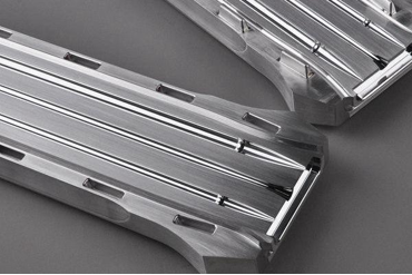 The following is a comparative analysis of the impact of different levels of surface finish on semiconductor applications:
Surface Roughness (Ra) | Application Level | Performance Impact | Risk Level |
0.8 μm | Standard precision sealing components | Meets basic structural and assembly requirements | Low |
0.4 μm | High-precision packaging components | Improved sealing performance and stability | Medium |
≤ 0.2 μm | High-end semiconductor equipment components | Near mirror finish, reduces particle contamination | High requirement |
To achieve this level of surface quality, systematic optimization needs to be carried out from multiple aspects. Firstly, the rigidity and stability of the CNC equipment itself are crucial. High-speed spindles and low-vibration structures form the foundation; otherwise, any micro-vibration will directly be reflected on the surface texture. Secondly, the selection of cutting tools is important. Ultra-sharp carbide or PCD diamond cutting tools can significantly reduce cutting tearing and improve surface consistency.
In terms of processing strategies, a high rotational speed, small cutting depth, and stable feed rate should be adopted to avoid surface shock caused by intermittent cutting. At the same time, five-axis processing can reduce the number of clamping operations and positioning errors, enabling the acquisition of a more uniform surface quality for curved surfaces or complex structures. Moreover, the cooling system is equally crucial. Micro-lubrication (MQL) or air cooling methods can effectively reduce thermal deformation and prevent surface oxidation or deterioration.
The influence of different processes on surface quality can be summarized as follows:
Control Factor | Key Function | Impact on Surface Finish |
CNC Machine Rigidity | Suppresses vibration | Determines the upper limit of base surface quality |
Tooling System | Ensures cutting stability | Directly affects surface texture and smoothness |
Machining Parameters | Controls cutting behavior | Manages roughness variation and consistency |
Reduces setup and clamping errors | Improves overall consistency and accuracy | |
Cooling Method | Controls thermal deformation | Prevents surface damage and oxidation |
Post-Processing | Surface refinement | Achieves mirror-level finish |
Finally, post-processing techniques such as precision polishing, electrochemical polishing or anodizing can further enhance the surface quality, making it meet the standards for semiconductor applications. At the same time, throughout the entire processing procedure, cleanliness control is also of great importance to avoid the influence of oil stains, metal particles or environmental pollution on the final surface performance.
Overall, achieving ultra-fine surface smoothness in semiconductor packaging is essentially a process of collaborative optimization involving "equipment, process, materials, and environment". Only when each aspect is controlled to a high standard can the strict requirements of the high-end semiconductor industry be truly met.
5.How To Handle Custom Semiconductor Enclosures With Extreme Geometry
Extreme geometry in semiconductor parts is no longer a barrier. Modern designs often require features that seem impossible to produce. Think of deep undercuts, complex internal cavities, or incredibly thin walls.
This is where CNC machining becomes the essential solution. It offers precision and control that other methods can’t match. For custom CNC enclosures, this capability is critical. It transforms radical concepts into functional, high-performance components.
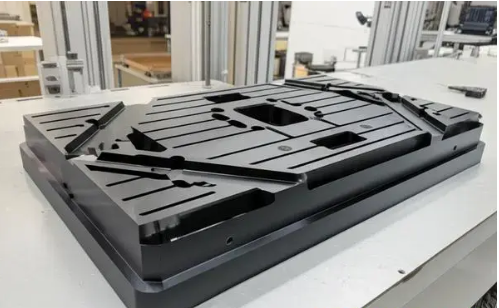 The CNC Machining Advantage
CNC provides direct solutions for challenging designs.
Precision is everything in semiconductor housing machining. Complex designs are not just for looks; they are for function. They manage heat, shield from interference, and fit into tight spaces. CNC machining directly addresses these needs.
Mastering Complex Geometries
Multi-axis CNC machines are key. They allow the cutting tool to approach the workpiece from many different angles.
Undercuts and Internal Cavities
Creating undercuts and internal shapes is straightforward with 5-axis machining. The machine tool can tilt and rotate. This eliminates the need for multiple setups, which saves time and reduces the risk of errors. A precise toolpath10 is programmed to navigate these complex internal features perfectly.
Achieving Thin, Rigid Walls
Thin walls require a delicate balance. You need strength without bulk. Our approach combines advanced material knowledge with optimized cutting strategies. We use high-speed milling with very sharp tools. This minimizes cutting forces and prevents the thin walls from deforming during the process.
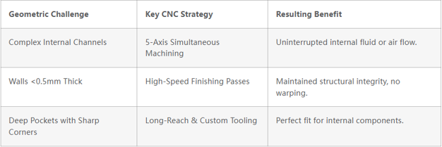
This detailed control ensures every feature, no matter how small or complex, is produced exactly as designed.
Advanced CNC machining is the definitive solution for semiconductor enclosures with extreme geometries. It enables the creation of undercuts, internal cavities, and thin walls with high precision, turning complex designs into reality without compromising on quality or functional requirements.


